
Contents
Features...................................................................................................1
Applications..............................................................................................1
Package Name ........................................................................................1
Block Diagram..........................................................................................2
The meaning of product model number ...................................................3
Selection Guide........................................................................................3
Pin Assignment ........................................................................................4
Absolute Maximum Ratings......................................................................4
Electrical Characteristics (1).....................................................................5
Electrical Characteristics (2) ....................................................................6
Electrical Characteristics (3).....................................................................7
Electrical Characteristics (4).....................................................................7
Measurement Circuits ..............................................................................8
Description of Operation ........................................................................ 10
Operation Timing Chart.......................................................................... 16
Battery Protection IC Connection Example ............................................ 19
Precautions ............................................................................................
20
Characteristic (typical characteristic)...................................................... 21
Dimensions ............................................................................................ 24

Rev.3.2
Seiko Instruments Inc.
1
BATTERY PROTECTION IC (FOR A SINGLE-CELL PACK)
S-8241 Series
The S-8241 is a series of lithium-ion/lithium polymer rechargeable
battery protection ICs incorporating high-accuracy voltage detection
circuits and delay circuits.
These ICs are suitable for protection of single-cell lithium ion/lithium
polymer battery packs from overcharge, overdischarge and overcurrent.
!"
!"
!"
!"
Features
(1) Internal high-accuracy voltage detection circuit
!" Overcharge detection voltage
3.9 V to 4.4 V (5 mV-step)
Accuracy of
� 25 mV(+25#C) or
� 30 mV(-5#C to +55#C)
!" Overcharge release voltage
3.8 V to 4.4 V (*1)
Accuracy of � 50 mV
*1: Overcharge release voltage = Overcharge detection voltage - Overcharge hysteresis
The overcharge hysteresis can be selected in the range 0.0, or 0.1 to 0.4 V in 50mV steps.
(However, selection "Overcharge release voltage<3.8 V" is impossible.)
!" Overdischarge detection voltage 2.0 V to 3.0 V (100 mV-step) Accuracy of � 80 mV
!" Overdischarge release voltage
2.0 V to 3.4 V (*2)
Accuracy of � 100 mV
*2: Overdischarge release voltage = Overdischarge detection voltage + Overdischarge hysteresis
The overdischarge hysteresis can be selected in the range 0.0 to 0.7 V in 100mV steps.
(However, selection "Overdischarge release voltage
$3.4 V" is impossible.)
!" Overcurrent 1 detection voltage
0.05 V to 0.3 V (5 mV-step)
Accuracy of � 20 mV
!" Overcurrent 2 detection voltage
0. 5 V (fixed)
Accuracy of � 100 mV
(2) A high voltage withstand device is used for charger connection pins (VM and CO pins: Absolute
maximum rating = 26 V)
(3) Delay times (overcharge: tCU; overdischarge: tDL; overcurrent 1: tlOV1; overcurrent 2: tlOV2) are
generated by an internal circuit. (External capacitors are unnecessary.) Accuracy of � 30 %
(4) Internal three-step overcurrent detection circuit (overcurrent 1, overcurrent 2, and load short-circuiting)
(5) Either the 0V battery charging function or 0V battery charge inhibiting function can be selected.
(6) Versions with and without a power-down feature can be selected.
(7) Charger detection function and abnormal charge current detection function
!" The overdischarge hysteresis is released by detecting a negative VM pin voltage (typ. -1.3 V).
(Charger detection function)
!" If the output voltage at DO pin is high and the VM pin voltage becomes equal to or lower than the
charger detection voltage (typ. -1.3 V), the output voltage at CO pin goes low. (Abnormal charge
current detection function)
(8) Low current consumption
!" Operation
3.0 %A typ.
5.0 %A max.
!" Power-down mode 0.1 %A max.
(9) Wide operating temperature range:
-40 to +85 #C
(10) Small package
SOT-23-5 (5-pin), SON-5 (5-pin)
!
!
!
! Applications
!
!
!
!
Package Name
!" Lithium-ion rechargeable battery packs
! SOT-23-5 (5-pin) (PKG drawing code : MP005-A)
!" Lithium- polymer rechargeable battery packs
! SON-5 (5-pin) (PKG drawing code : PN005-A)

BATTERY PROTECTION IC FOR A SINGLE-CELL PACK
Rev.3.2
S-8241 Series
2
Seiko Instruments Inc.
!
Block Diagram
+
&
&
+
VM
VSS
VDD
CO
DO
Overcharge
detection
comparator
Overcurrent 1
detection comparator
&
+
&
+
Level conversion circuit
0V battery/charging circuit
'/charge inhibition circuit
Load short-
circuiting
detection circuit
Overdischarge
detection
comparator
Overcurrent 2
detection comparator
Delay circuit
RVMD
RVMS
Counter circuit
Clock generation circuit
Charger
detection circuit
The overdischarge hysterisis
is released when a charger is
detected.
RCOL
Note: The diode in the IC is a parasitic diode.
"
Figure 1 Block Diagram
Rev.3.2
BATTERY PROTECTION IC FOR A SINGLE-CELL PACK
S-8241 Series
Seiko Instruments Inc.
3
!"
!"
!"
!"
The meaning of product model number
Model number: S-8241AB
(
(
(
(##
##
##
##-product abbreviation (GB
(
(
(
()-reel orientation (T2 or TF)
Symbol
Meaning
Description
(
Serial number
Is set from A to Z in sequence.
##
Package form
MC:SOT-23-5, PN:SON-5
!"
!"
!"
!"
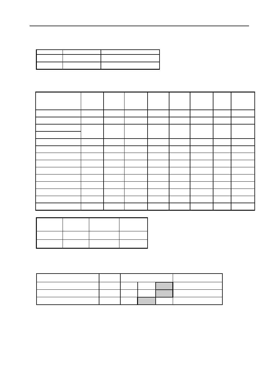
Selection Guide
Model No./Item
Over-
charge
detection
voltage
Over-
charge
release
voltage
Over-
discharge
detection
voltage
Over-
discharge
release
voltage
Over-
current 1
detection
voltage
0V battery
charging
function
Delay
time
combi-
nation*
Power
down
feature
S-8241ABAMC-GBA-T2
4.275 V
4.075 V
2.3 V
2.9 V
0.100 V
unavailable
(1)
Available
S-8241ABCMC-GBC-T2
4.350 V
4.100 V
2.3 V
2.8 V
0.075 V
unavailable
(1)
Available
S-8241ABDMC-GBD-T2
4.275 V
4.175 V
2.3 V
2.4 V
0.100 V
available
(1)
Available
S-8241ABDPN-KBD-TF
S-8241ABEMC-GBE-T2
4.295 V
4.095 V
2.3 V
3.0 V
0.200 V
unavailable
(1)
Available
S-8241ABFMC-GBF-T2
4.325 V
4.075 V
2.5 V
2.9 V
0.100 V
unavailable
(1)
Available
S-8241ABGMC-GBG-T2
4.200 V
4.100 V
2.3 V
3.0 V
0.100 V
unavailable
(1)
Available
S-8241ABHMC-GBH-T2
4.325 V
4.125 V
2.3 V
2.3 V
0.100 V
available
(1)
Available
S-8241ABIMC-GBI-T2
4.280 V
4.080 V
2.3 V
2.3 V
0.160 V
unavailable
(1)
Available
S-8241ABKMC-GBK-T2
4.325 V
4.075 V
2.5 V
2.9 V
0.150 V
unavailable
(1)
Available
S-8241ABLMC-GBL-T2
4.320 V
4.070 V
2.5 V
2.9 V
0.100 V
unavailable
(1)
Available
S-8241ABNPN-KBN-TF
4.350V
4.050V
2.35V
2.65V
0.150V
available
(1)
Available
S-8241ABOMC-GBO-T2
4.350V
4.15V
2.3V
3.0V
0.150V
available
(2)
Available
S-8241ABPMC-GBP-T2
4.350V
4.15V
2.3V
3.0V
0.200 V
available
(2)
Available
*The delay time combination (1), (2) is as follows.
Delay time
combination
Overcharge
detection
delay time
Overdischarge
detection
delay time
Overcurrent 1
detection
delay time
(1)
1.0 s
125 ms
8 ms
(2)
0.125s
31ms
16ms
It is possible to change the detection voltage for products other than those listed above. Also, delay time can be changed within the
following range. For details, please contact our sales office.
Delay time
Symbol
Optional range
Remarks
Overcharge detection delay time
tCU
0.25 s
0.5 s
1.0 s
Choose from the list at left.
Overdischarge detection delay time
tDL
31 ms
62.5 ms
125 ms
Choose from the list at left.
Overcurrent 1 detection delay time
tlOV1
4 ms
8 ms
16 ms
Choose from the list at left.
* Boxes in bold line indicate standard products.

BATTERY PROTECTION IC FOR A SINGLE-CELL PACK
Rev.3.2
S-8241 Series
4
Seiko Instruments Inc.
!"
!"
!"
!"Pin Assignment
For details of package, refer to the attached drawing.
Figure 2
Figure 3
!"
!"
!"
!"
Absolute Maximum Ratings
(Ta = 25#C unless otherwise specified)
Item
Symbol
Applicable pin
Rating
Unit
Input voltage between VDD
and VSS *
V
DS
VDD
V
SS
-0.3 to V
SS
+12
V
VM Input pin voltage
V
VM
VM
V
DD
-26 to V
DD
+0.3
V
CO output pin voltage
V
CO
CO
V
M
-0.3 to V
DD
+0.3
V
DO output pin voltage
V
DO
DO
V
SS
-0.3 to V
DD
+0.3
V
Power dissipation
P
D
SOT-23-5
250
mW
SON-5
150
Operating temperature range
Topr
-40 to +85
#C
Storage temperature range
Tstg
-40 to +125
#C
Note: This IC contains a circuit that protects it from static discharge, but take special care that no excessive static electricity or
voltage which exceeds the limit of the protection circuit is applied to the IC.
* Pulse
(
%sec) noise exceeding the above input voltage (V
SS
+ 12 V) may cause damage to the IC.
Pin No.
Symbol
Description
1
VM
Voltage detection pin between
VM and VSS
(Overcurrent detection pin)
2
VDD
Positive power input pin
3
VSS
Negative power input pin
4
DO
FET gate connection pin for
discharge control
(CMOS output)
5
CO
FET gate connection pin for
charge control (CMOS output)
1
SOT-23-5
Top view
2
3
5
4
Pin No.
Symbol
Description
1
VM
Voltage detection pin between
VM and VSS
(Overcurrent detection pin)
2
VDD
Positive power input pin
3
CO
FET gate connection pin for
charge control (CMOS output)
4
DO
FET gate connection pin for
discharge control
(CMOS output)
5
VSS
Negative power input pin
4
5
3
2
1
SON-5
Top view